


What is the difference between the first and 2. three generations of semiconductors?
Release time:
2020-06-19
Semiconductor raw materials have gone through three stages of development: the first stage is based on silicon (Si), germanium (Ge) as the first generation of semiconductor raw materials; the second stage is based on gallium arsenide (GaAs), indium phosphide (InP) and other compounds; the third stage is based on gallium nitride (GaN), silicon carbide (SiC), zinc selenide (ZnSe) and other broadband semiconductor raw materials.
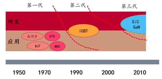
History of Semiconductor Materials and Devices
In the field of materials, the first generation, the second generation, the third generation does not have“The latter generation is better than the previous generation”The statement. Materials such as gallium nitride and silicon carbide are generally called wide band gap semiconductors abroad; gallium nitride, aluminum nitride, indium nitride and their mixed crystal materials become nitride semiconductors, or gallium nitride, gallium arsenide and indium phosphide becomeIII-VGroup semiconductors. The third generation of semiconductor materials adopted in China corresponds to the three industrial revolutions brought about by the large-scale application of semiconductor materials in human history. At present, the third-generation semiconductors are developing at a high speed, and the first and second-generation semiconductors are still used on a large scale in the industry, playing an irreplaceable role in the third-generation semiconductors. What progress does the third generation semiconductor have compared with the first generation and the second generation? What are the technical differences between these three generations of semiconductors? Why is gallium nitride(GaN)and silicon carbide(SiC)Highly sought after in third-generation semiconductors?
01
First Generation Semiconductor Materials
Rise timein the 1950 s;
Representative Materials: Silicon (Si), germanium element (Ge) Semiconductor materials.
historical significance: The first generation of semiconductor materials gave rise to integrated circuits (IC) as the core of the rapid development of microelectronics. Due to the narrow band gap of silicon material, the low electron mobility and breakdown electric field,SiApplications in the field of optoelectronics and high-frequency high-power devices are subject to many limitations. However, the first generation of semiconductors have high technological maturity and cost advantages, and are still widely used in the field of electronic information and new energy and silicon photovoltaic industries.
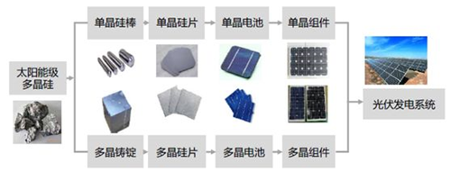
Silicon application industry chain in the field of photovoltaic
02
Second Generation Semiconductor Materials
Rise time:20Since the nineties of the century,With the rapid development of mobile communication, the rise of the information superhighway based on optical fiber communication and the Internet,Gallium arsenide, indium phosphide as the representative of the second generation of semiconductor materials began to emerge.
Representative Materials: The second-generation semiconductor materials are compound semiconductors; such as gallium arsenide (GaAs), indium antimonide (InSb);GaAsAl,GaAsP; and some solid solution semiconductors, suchGe-Si,GaAs-GaPGlass semiconductors (also known as amorphous semiconductors), such as amorphous silicon, glassy oxide semiconductors; organic semiconductors, such as phthalocyanine, copper phthalocyanine, polyacrylonitrile, etc.
Performance characteristicsCompared with the first generation of semiconductors, gallium arsenide has the characteristics of high frequency, radiation resistance and high temperature resistance, so it is widely used in mainstream commercial wireless communication, optical communication and national defense industry.
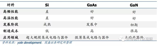
historical significance: The second generation semiconductor materials are mainly used to make high-speed, high-frequency, high-power and light-emitting electronic devices, and are excellent materials for making high-performance microwave, millimeter wave devices and light-emitting devices. Due to the rise of the information superhighway and the Internet, it is also widely used in satellite communications, mobile communications, optical communications andGPSareas such as navigation. For example, compared to the first generation of semiconductors, gallium arsenide (GaAs) can be applied in the field of optoelectronics, especially in infrared lasers and high-brightness red diodes.
From21At the beginning of the 21st century, smart phones, new energy vehicles, robots and other emerging electronic technologies have developed rapidly. At the same time, the global energy and environmental crisis is prominent, and energy utilization tends to be low power consumption and fine management. The traditional first and second generation semiconductor materials have been unable to meet the needs of science and technology due to their own performance limitations, which calls for the emergence of new materials to replace them.
03
third generation semiconductor materials
Time of OriginThe United States was earlier.1993The first gallium nitride materials and devices have been developed in, and the earliest research team in China——Institute of Semiconductors, Chinese Academy of Sciences1995Research in this area was also initiated in2000years made.HEMTStructural materials.
Representative Materials: The third generation of semiconductor materials are mainly silicon carbide (SiC), gallium nitride (GaN), zinc oxide (ZnO), diamond, aluminum nitride (AlN) as the representative of the wide band gap (Eg》2.3eV) Semiconductor materials.
development status: in5GUnder the clear traction of application requirements such as communications, new energy vehicles, and photovoltaic inverters, the head companies in the application field have begun to use third-generation semiconductor technology, which has further boosted industry confidence and firm investment in the third-generation semiconductor technology route.
Performance analysis: Compared with the first and second generation semiconductor materials, the third generation semiconductor materials have a wider band gap(>2.2eV), higher breakdown electric field, higher thermal conductivity, higher electron saturation rate and higher radiation resistance, more suitable for the production of high temperature, high frequency, high power and radiation resistance devices, can be widely used in high voltage, high frequency, high temperature and high reliability and other fields, including radio frequency communication, radar, satellite, power management, automotive electronics, industrial power electronics, etc.
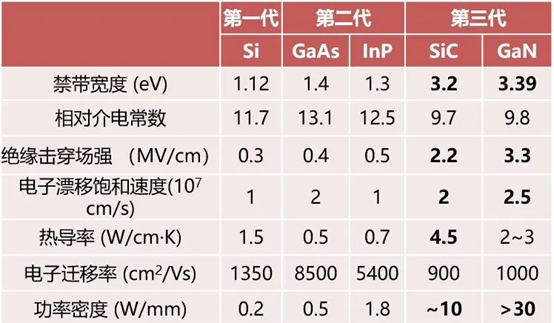
Comparison of Main Performance Parameters of Semiconductor Materials
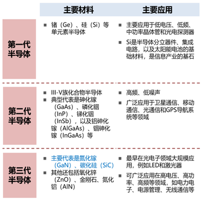
Main Materials and Applications of Semiconductors
In the third generation of semiconductors,SiCwithGaNIn comparison, the former is relativelyGaNThe development is earlier and the technological maturity is higher; one big difference between the two is thermal conductivity, which makes it possible in high-power applications,SiCdominant position; at the same time dueGaNIt has a higher electron mobility and thus can be comparedSiCorSiWith higher switching speed, in high frequency applications,GaNHave advantages.
From the following table commonly used“Superior Value (Figure of Merit, FOM)”It can be clearly seen that,SiCandGaNCompared with the previous two generations of semiconductor materials, the functions and characteristics have been greatly improved.
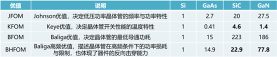
*The above merit value is based onSiMaterial as Unit1, normalized
GaNandSiCEach has its own advantages and disadvantages in material performance, so it has its own emphasis and complementarity in the application field. SuchGaNof high frequencyBaligaThe merit is significantly higherSiC, thereforeGaNadvantages in the field of high-frequency small power, focusing on1000VHereinafter, for example, a communication base station, a millimeter wave, etc.SiCofKeyeThe merit is significantly higherGaN, thereforeSiCThe advantages of high temperature and1200VThe above large power fields include electric power, high-speed rail, electric vehicles, industrial motors, etc. In the low and medium frequency, low and medium power fields,GaNandSiCcan be applied, with the traditionalSiBase device competition.
Third-generation semiconductors-Gallium Nitride(GaN)
GaNThe devices mainly include RF devices, power electronic power devices, and optoelectronic devices.GaNThe commercial applicationLEDlighting and lasers, which are more based onGaNdirect band gap characteristics and spectral characteristics, related industries have developed very mature. RF devices and power devices play aGaNMain application fields of wide band gap semiconductor characteristics.
Application advantages: small size, high frequency and high power, low energy consumption and fast speed;5GCommunication will beGaNKey growth drivers for the RF devices market.
5GThe base station will use multiple-and-receive antenna array solutions,GaNRF devices provide a huge improvement in the power consumption and size of the entire antenna system. In high-power, high-frequency RF applications, higher bandwidth, faster transmission rates, and lower system power consumption,GaNRF power transistor as a new solid-state energy microwave source, replacing the traditional2.45GHzMagnetrons are used in consumer electronics and industrial applications, from microwave ovens to high-power welding machines.
2017The size of the global power semiconductor market in327Billions of dollars, expected2022Year reached426Billions of dollars. Industrial, automotive, wireless communications and consumer electronics are the top four end markets.
Third-generation semiconductors-Silicon Carbide(SiC)
SiCFrom the last century70The research and development began in the s.2001YearSiCSBDCommercial,2010YearSiCMOSFETCommercial.SiCIGBTIt is currently under development.SiCIt can greatly reduce the switching loss in power conversion, so it has better energy conversion efficiency, it is easier to realize the miniaturization of the module, and it is more resistant to high temperature.
SiCThe main application of power devices: Smart grid, transportation, new energy vehicles, photovoltaic, wind power;New energy vehicles areSiCKey Growth Drivers for the Power Devices Market. CurrentlySiCThe application of devices in new energy vehicles is mainly power control units.(PCU)Inverter,Alcatel re-stockingConverter, car charger, etc.
2017Global YearSiCTotal power semiconductor market3.99Billions of dollars. expected2023year,SiCThe total market for power semiconductors will reach16.44Billions of dollars.
04
Summary
Long-term coexistence of first and second generation semiconductor technologiesAt this stage, the first and 2. three generations of semiconductor materials are widely used. Why did the second generation not replace the first generation? Can the third generation of semiconductors fully replace traditional semiconductor materials?
That's becauseSiand compound semiconductors are two complementary materials, and certain performance advantages of the compound compensate forSidisadvantages of the crystal, whileSiThe crystal production process has obvious irreplaceable advantages, and both have certain limitations in the application field. Therefore, in the application of semiconductors, compatible means are often used to make the two compatible, taking their respective advantages, so as to produce products that meet higher requirements, such as high reliability and high speed national defense military products. Therefore, the first and second generations are a long-term common state.
The third generation is expected to replaceThe third generation of wide band gap semiconductor materials can be widely used in various fields, such as consumer electronics, lighting, new energy vehicles, missiles, satellites, etc., and has many excellent properties to break through the development bottleneck of the first and second generation semiconductor materials. Therefore, while being optimistic about the market, with the development of technology, it is expected to replace the first and second generation semiconductor materials in an all-round way.
New infrastructure provides huge development opportunities for domestic semiconductor manufacturers: China's start in the third semiconductor materials is relatively late, and the level of technology is relatively low compared to foreign countries. This is an opportunity to overtake in a corner, but there are still many difficulties and challenges that our country needs to face.
4Month20Day, the National Development and Reform Commission's first official announcement.“New Infrastructure”The scope of the, officially set the tone5GInfrastructure, artificial intelligence, industrial Internet and other seven areas of development direction.“New Infrastructure”As an emerging industry, one end is connected with the ever-upgrading consumer market, and the other end is connected with the rapid development of scientific and technological innovation. It is worth noting that either5G, new energy vehicles or industrial Internet, etc,“New Infrastructure”The construction of various industries is closely related to the development of semiconductor technology. For example: with gallium nitride(GaN)as the core of the RF semiconductor, supporting5GConstruction of base stations and industrial Internet systems; silicon carbide(SiC)andIGBTAs the core of the power semiconductor, supporting new energy vehicles, charging piles, base stations./Construction of data center power supplies, UHV and rail transit systems;AIChip as the coreSOCChips support the construction of data centers and artificial intelligence systems.
It is not difficult to see that gallium nitride(GaN)and silicon carbide(SiC)The third generation of semiconductors is supported“New Infrastructure”The core material. In“New Infrastructure”With the blessing of domestic substitution, domestic semiconductor manufacturers will usher in huge development opportunities.
Related News
Guo Yuansheng: Sensors will become the new focus of international strategic competition
The current pace of development of the digital economy is surprising. The U.S. digital economy totaled $10.83 trillion billion in 2017, accounting for more than 58.3 percent of GDP. It reached $12.34 trillion billion in 2018, accounting for more than 62% of GDP. China followed closely, with the digital economy of more than $34000 billion, or 30.3 per cent of GDP, in 2017 and more than $47300 billion, or 34.8 per cent of GDP, in 2018. China and the United States already account for more than 50% of the global digital economy.
2020-07-02
On the morning of July 9, the Intelligent Equipment Industry Development Center of the High-tech Zone, in conjunction with the East District Sub-district Office, held a land acquisition and demolition coordination meeting in the sub-district office conference room to study and solve the problem of land demolition on the Shandong Huaco project. Ling Ning, deputy director of the Intelligent Equipment Industry Development Center, Zhai Jianxin, deputy secretary of the Party Working Committee of the Eastern District Sub-district Office, and Feng Haiying, director and deputy general manager of Shandong Huaco, attended the meeting.
2020-07-10
On the afternoon of July 9, Wang Chong, deputy director of Jinan Municipal Bureau of Industry and Information Technology, and Guo Jingmin, deputy inspector, visited our company for investigation. General Manager Ge Jiannan received the research group.
2020-07-10
On July 27, in the production workshop of Shandong Huake Semiconductor Research Institute Co., Ltd. (hereinafter referred to as "Shandong Huake") located in Jinan High-tech Zone, the temperature sensor chip HK1020, which was independently designed and developed by Shandong Huake and can completely replace the imported temperature sensor chip, was officially put into mass production after grinding, crystal fixing, wire bonding, packaging, testing and calibration. HK1020 chip, actually only millet grain size this hk1020 chip only millet grain big. "Don't underestimate this'little rice grin'. It contains dozens of layers of circuit boards and requires dozens of photolithography. It has high temperature measurement accuracy and sensitive response." Shandong Huako production and technical personnel Jin Hangfei said. The HK1020 temperature sensor chip can provide a measurement resolution of 9~12 bits, its temperature measurement range is -55 ℃ ~ +125 ℃, and its temperature measurement accuracy is ± 0.5 ℃ in the range of -10 ℃ ~ +85 ℃, which is suitable for various temperature control systems. "Compared with the similar product 18B20, which had a monopoly position in the world before, our product has better temperature measurement accuracy and 20% lower price. It is fully capable of replacing similar foreign products." Shandong Huako marketing department head said. Shandong Huako HK1020 temperature sensor chip has just been mass produced. 35 customers in Shandong and 27 customers in Shenzhen have come to order. Shandong Huaco has another 2 new temperature sensors to be launched soon. The first temperature and humidity sensor chip has also been designed and will be mass produced by the end of the year. Application of sensors in mobile phones and bracelets Sensor chips are closely related to people's lives. Air conditioning automatically adjusts temperature and humidity, reversing radar perceives things, mobile phone face recognition, unmanned driving, etc., are all inseparable from sensors. "Sensors are like human eyes, nose, ears, and skin. Its sensitivity determines the sensitivity of smart terminals." Ge Jiannan, general manager of Shandong Huaco, revealed that at present, the scale of China's sensor chip market exceeds 200 billion yuan and continues to grow at a high speed. Due to the late start of technology, it has been monopolized by foreign enterprises. Shandong Huako Production Workshop In May 2018, with the help of the technical cooperation advantages of the Semiconductor Research Institute of the Chinese Academy of Sciences, Shandong Huaco was registered and established in Jinan High-tech Zone. The company's research and development team to accelerate the transformation of technological achievements, currently has detection, small signal amplification, analog-to-digital conversion, calibration algorithms and other invention patents, integrated circuit layout protection and software copyright. Shandong Huako has completely independent intellectual property rights to the first temperature sensor HK1020. Shandong Huako High Precision Digital Smart Sensor Project is listed as a major project in Shandong Province in 2020. They are committed to building China (Jinan) Smart Sensor Valley and promoting the development of sensor chip industry chain clusters. "We strive to 3-5 years to the Chinese 'core' brand to the world." Ge Jiannan introduced. Planning of Shandong Huako High Precision Sensor Industrial Park Reporter: Li Mengmeng Correspondent: Wang Pengfei Editor: Zhao Qian Source: Jinan Daily
2020-07-29
On the morning of July 31, Gao Fang, member of the party group and deputy director of the Shandong Provincial Department of Industry and Information Technology, and his party went to Shandong Huake for investigation. Shi Zhenyuan, member of the Standing Committee of the Party Committee and deputy general manager of Shandong Expressway Group, received the research team.
2020-08-01
Contact Us
> Address: F7-2-201-203, innovation works, 2016 Feiyue Avenue, High-tech Zone, Jinan City, Shandong Province
> Marketing Department:+86-531-55770800
> Operator:+86-531-55770700
Sweep, pay attention to us
Copyright:Shandong Huake Semiconductor Research Institute Co., Ltd. Technical Support:300.CN Jinan2 Seo 【Business license】